Spatial dependence of the superconducting order parameter
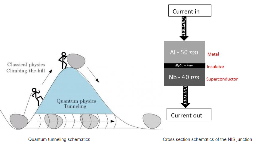
In an effort to study the spatial dependence of the superconducting order parameter we plan using Normal/Insulator/Superconducting junction exhibiting quantum tunneling effect. 'Quantum tunneling' refers to a phenomenon where a particle tunnels through a barrier that it classically cannot occur. It has important applications to modern devices such as the tunnel diode, quantum computing, and the scanning tunneling microscope (STM).

For the present research, we fabricate a Normal Metal-Insulator-Superconductor (NIS) junctions and measure the electron tunneling as a function of the voltage applied. The fabrication process includes Electron-beam lithography (EBL), Atomic Layer Deposition (ALD), DC-Magnetron sputtering and Electron-beam physical vapor deposition. The right figure shows Scanning Electron Microscope (SEM) image of Al-Al2O3-Nb junction where Al is the normal metal, Al2O3 is the insulator and the Nb is the superconductor.


